

Interfaces and Hardware Layout
There are two reference systems for the developer kit: the numbered labels (0–12) on the side views, used by NVIDIA's official guide and by this page, and the carrier-board connector numbers (J-numbers) printed on the PCB. Keep both handy — the rest of our guides refer to them.
Side views — labeled parts
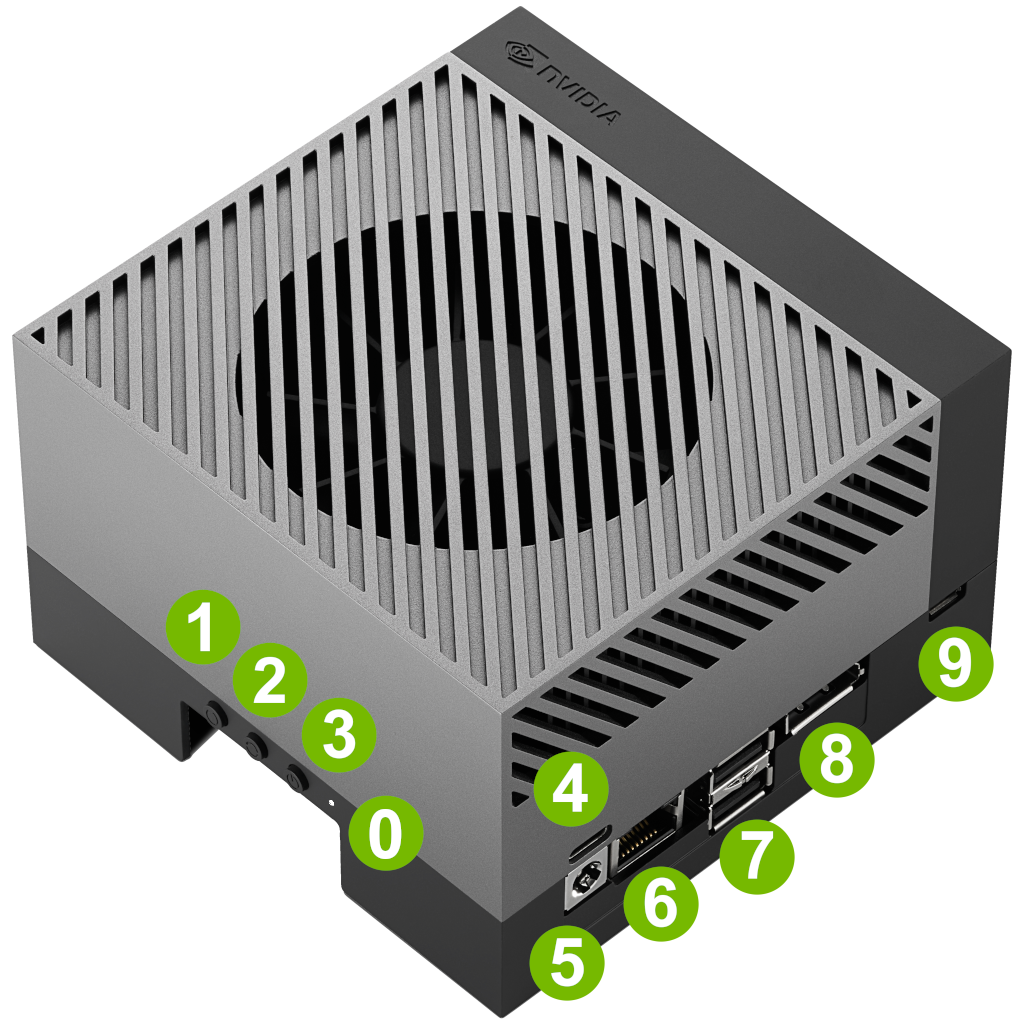
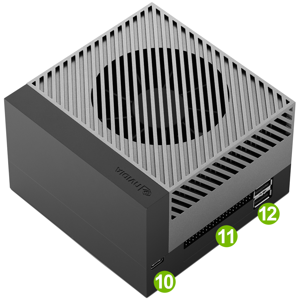
| # | Part | Notes |
|---|---|---|
| 0 | White LED | Power indicator |
| 1 | Power button | |
| 2 | Force Recovery button | Used for recovery / flash modes |
| 3 | Reset button | |
| 4 | USB Type-C port | DFP only (connect peripherals) |
| 5 | DC power jack | Barrel jack — see J41 for the spec |
| 6 | Ethernet port | |
| 7 | USB Type-A ×2 | USB 3.2 Gen 2 |
| 8 | DisplayPort output | The only display interface on the kit |
| 9 | USB micro-B port | For debug |
| 10 | USB Type-C port | Flashing and data (UFP and DFP) |
| 11 | 40-pin connector | |
| 12 | USB Type-A ×2 | USB 3.2 Gen 1 |
Carrier board — connectors
| Mark | Connector | Specification / notes |
|---|---|---|
| DS2 | White LED | |
| S1 / S2 / S3 | Power / Reset / Force Recovery buttons | |
| J24 | USB Type-C (above DC jack) | DFP only, USB 3.2 Gen 2 — this is where the included USB-C power supply connects |
| J41 | DC power jack | 5.5 mm OD, 2.5 mm ID, center positive |
| J17 | Ethernet | Up to 10GBASE-T |
| J33 | USB Type-A ×2 (next to Ethernet) | USB 3.2 Gen 2 |
| J18 | DisplayPort output | Supports MST |
| J26 | USB micro-B | Debug UART |
| J40 | USB Type-C (next to 40-pin header) | UFP and DFP — the port used to connect to a host PC for SDK Manager |
| J30 | 40-pin connector | Pin 1 is marked with a white triangle on the PCB |
| J42 | Automation header | Auto power-on, wake-on-LAN, throttling trigger (pins below) |
| J13 | RTC backup battery connector | |
| J509 | Camera connector | |
| J502 | JTAG debug connector | |
| J505 | M.2 E-Key slot | Typically holds the Wi-Fi module |
| J511 | HD Audio header | |
| J1 | M.2 M-Key slot | For an NVMe SSD |
| J10 | microSD card slot | UHS-1 |
| J3 | Jetson module connector | 699-pin |
| J6 | PCIe x16 connector | PCIe 4.0 ×8 electrically |
| J9 | Fan connector | 4-pin, 1.25 mm pitch |
The three things people ask about first:
- Display: DisplayPort (J18) is the only display output — there is no HDMI port and no DisplayPort-over-USB-C. For an HDMI monitor, use an active DP→HDMI adapter or cable.
- Power: the included USB-C power supply connects to J24 (the USB-C port above the DC jack). A separate barrel-jack input (J41) is available if you supply your own power.
- Host-PC connection: for SDK Manager or a serial console, use J40 (the USB-C port next to the 40-pin header) — not J24.
DisplayPort output
- Supports DP SST, DP MST (up to 2 external displays), and DP DSC
- Max resolution: 8K@30 / 4K@120 (with or without DSC)
- Output formats: RGB 8/10 bpc, YUV444 8/10 bpc
Storage options
- Default: eMMC flash memory on the module
- Optional: NVMe SSD (M.2 M-Key, J1) · microSD card (J10, UHS-1) · USB drive
The Jetson ISO installer can install the system to eMMC or NVMe; SDK Manager can flash the base L4T BSP to any of the supported storage media.
40-pin header (J30)
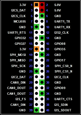 40-pin header pinout — from NVIDIA's Carrier Board Specification.
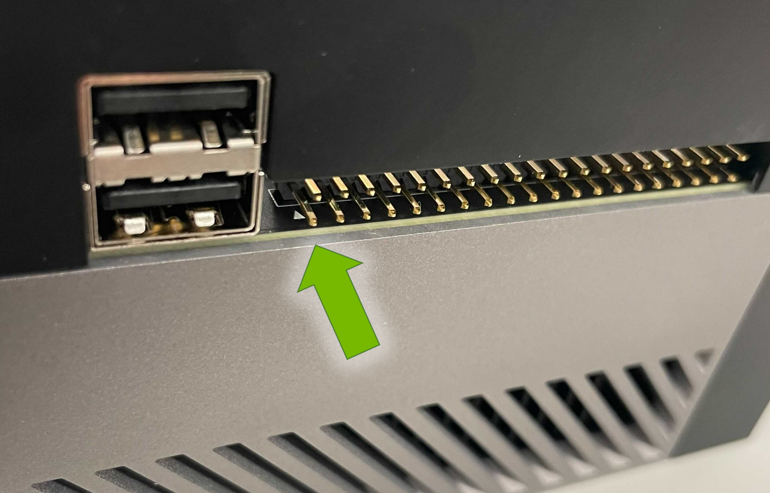 Pin 1 is marked with a white triangle on the PCB.
Automation header (J42)
Used for production and automation wiring:
- Pin 1, 12: GND
- Pin 2, 3, 4: inputs, same function as the Recovery, Reset, and Power buttons
- Pin 5–6: open = auto power-on disabled; short = auto power-on enabled
- Pin 7: CVB_STBY output — indicates whether the module is in sleep
- Pin 8: SYSTEM_OC input — triggers Tegra throttling
- Pin 9–10: open = wake/boot-on-LAN from off disabled; short = enabled
- Pin 11: JTAG_TRST — JTAG test reset
Sources
- Hardware Layout — Jetson AGX Orin Developer Kit User Guide (checked 2026-09-23)
- For carrier-board details, see the NVIDIA Jetson AGX Orin Developer Kit Carrier Board Specification (linked from NVIDIA's downloads page)
Status: draft, pending review by cheny. Steps and values above are grounded in NVIDIA's official documentation as of the date listed; not yet verified on physical hardware by Juxi Technology.
Image credits: Layout diagrams and pinout images are from NVIDIA's official Jetson AGX Orin Developer Kit User Guide and Carrier Board Specification (downloaded 2026-09-23) and remain © NVIDIA Corporation.
NVIDIA® and Jetson™ are trademarks of NVIDIA Corporation. This page is published by Juxi Technology and is not an NVIDIA publication.