

ESP32-NanoCam Hardware Spec
1. Hardware Overview
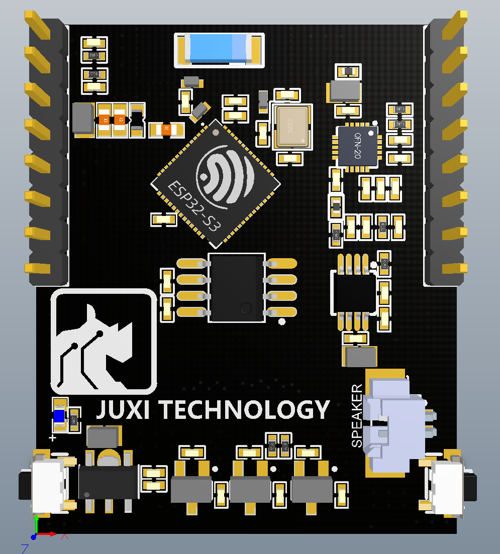
The hardware material in this section comes from the NanoCamModule.pdf + NanoCamBASE.pdf schematics. Overall architecture: the core board (ESP32-S3 + camera + audio) plugs onto the base board (USB power + serial flashing).
Plaintext
┌─────────────────────────────────────────────────────────┐
│                    NanoCam 核心板                         │
│  ┌──────────┐  ┌──────────┐  ┌────────────┐            │
│  │ ESP32-S3 │  │ ES8311   │  │ NS4150B   │            │
│  │   R8     │  │ I2S 麦克风│  │ I2S 功放   │            │
│  │ (QFN56)  │  │          │  │            │            │
│  └────┬─────┘  └──────────┘  └────────────┘            │
│       │                                                 │
│  ┌────┴─────┐  ┌──────────┐  ┌────────────┐            │
│  │ GD25Q128 │  │  DVP     │  │ ME6217C33  │            │
│  │ 16MB Flash│ │ 摄像头   │  │ 3.3V LDO   │            │
│  └──────────┘  │ FPC-24P  │  └────────────┘            │
│                └──────────┘                             │
├─────────────────────────────────────────────────────────┤
│                    NanoCam 底板                          │
│  ┌──────────┐  ┌──────────┐  ┌────────────────────┐    │
│  │ USB-C    │  │ CH340K   │  │ 一键下载电路        │    │
│  │ 5V输入   │  │ USB-UART │  │ (DTR/RTS→BOOT/EN)  │    │
│  └──────────┘  └──────────┘  └────────────────────┘    │
│                                                         │
│  扩展接口: I2C ×1, UART ×1, 5V/GND/3.3V                 │
└─────────────────────────────────────────────────────────┘
2. MCU and Storage
2.1 Main Chip
| Parameter | Specification |
|---|---|
| Model | ESP32-S3 N16R8 |
| Package | QFN56 |
| CPU | Xtensa LX7 dual-core 240MHz |
| PSRAM | 8MB (Octal SPI, R8 suffix) |
| Flash | 16MB (N16 suffix, external 128M-bit SPI Flash) |
| Clock | 40MHz passive crystal + 10pF×2 matching capacitors |
2.2 Flash Storage
| Parameter | Specification |
|---|---|
| Model | GD25Q128ESIG |
| Capacity | 128M-bit = 16MB |
| Interface | SPI (standard four-wire) |
| Brand | GigaDevice |
| Flash Signal | ESP32-S3 GPIO | Function |
|---|---|---|
| CS | IO29 | Chip select |
| SO (DO) | IO31 | Data output |
| SI (DI) | IO32 | Data input |
| SCLK | IO30 | Clock |
| WP | IO34 | Write protect |
| HOLD | IO33 | Hold |
3. Camera Subsystem
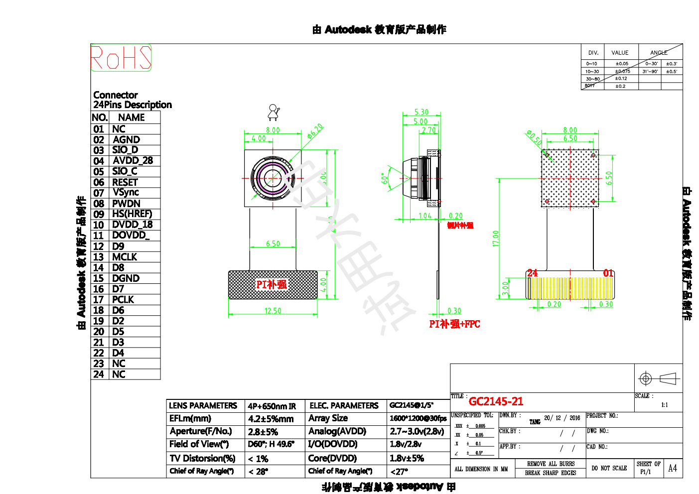
3.1 DVP Interface
| Parameter | Specification |
|---|---|
| Interface type | FPC 0.5 WS 24P (24-pin FPC connector) |
| Supported Sensors | GC2145 (default) / OV2640 / OV5640 and other DVP cameras |
| I2C configuration bus | SDA=IO41, SCL=IO42 (shared with the external I2C) |
| Pixel format | RGB565 / JPEG / YUV422, etc. |
3.2 Full DVP Pin Mapping
| Signal Category | Signal Name | ESP32 GPIO | Notes |
|---|---|---|---|
| System clock | XCLK | IO9 | Master clock output 24MHz |
| Pixel clock | PCLK | IO6 | Camera pixel clock input |
| Frame sync | VSYNC | IO13 | Vertical sync |
| Line sync | HREF | IO11 | Horizontal reference |
| Control | PWDN | IO12 | Camera power-down control |
| Control | RESET | IO14 | Camera reset |
| I2C | SDA | IO41 | Camera I2C data (shared with ES8311) |
| I2C | SCL | IO42 | Camera I2C clock (shared with ES8311) |
| Data D0 | Y2 | IO4 | Pixel data bit0 |
| Data D1 | Y3 | IO2 | Pixel data bit1 |
| Data D2 | Y4 | IO1 | Pixel data bit2 |
| Data D3 | Y5 | IO3 | Pixel data bit3 |
| Data D4 | Y6 | IO5 | Pixel data bit4 |
| Data D5 | Y7 | IO7 | Pixel data bit5 |
| Data D6 | Y8 | IO8 | Pixel data bit6 |
| Data D7 | Y9 | IO10 | Pixel data bit7 |
3.3 Camera Signal Group Summary
Plaintext
Camera DVP 信号组:
  XCLK  = IO9     # Master clock out (24MHz)
  PCLK  = IO6     # Pixel clock in
  VSYNC = IO13    # Vertical sync
  HREF  = IO11    # Horizontal ref
  PWDN  = IO12    # Power down (active low)
  RESET = IO14    # Hardware reset

  D0(Y2) = IO4    D1(Y3) = IO2
  D2(Y4) = IO1    D3(Y5) = IO3
  D4(Y6) = IO5    D5(Y7) = IO7
  D6(Y8) = IO8    D7(Y9) = IO10

  SIOD(SDA) = IO41
  SIOC(SCL) = IO42
4. Audio Subsystem
4.1 Audio Architecture
Plaintext
AP2718AT (模拟MEMS麦) → ES8311 Codec (ADC/DAC) → NS4150B (模拟功放) → 扬声器
                               ↕ I2S (MCLK=39,BCLK=38,WS=47,DOUT=48,DIN=40) + I2C (41/42, addr=0x30)
ESP32-S3| Component | Model | Type | Interface |
|---|---|---|---|
| Microphone | AP2718AT | Analog MEMS silicon microphone | Differential analog → ES8311 ADC |
| Codec | ES8311 | Audio codec (I2S+I2C) | I2S=MCLK=39,BCLK=38,WS=47,DOUT=48,DIN=40, I2C=41/42, addr=0x30 |
| Amplifier | NS4150B | Class-D analog amplifier | ES8311 DAC output → analog input → speaker |
4.2 ES8311 Codec I2S Pins
| I2S Signal | ESP32 GPIO | Function |
|---|---|---|
| MCLK | IO39 | Master clock |
| BCLK (SCLK) | IO38 | Bit clock |
| LRCLK (WS) | IO47 | Left/right channel clock |
| DOUT (DAC) | IO48 | Serial data output (playback) |
| DIN (ADC) | IO40 | Serial data input (recording) |
Audio uses I2S0 Standard Duplex mode; the ES8311 codec supports recording and playback simultaneously.
4.3 ES8311 I2C Control
| I2C Signal | GPIO | Description |
|---|---|---|
| SDA | IO41 | I2C bus shared with the camera |
| SCL | IO42 | I2C bus shared with the camera |
| Address | 0x30 | ES8311 8-bit I2C address |
5. Power System
5.1 Power Chain
Plaintext
USB-C (5V) ──→ 底板 NCE3401 P-MOSFET 反接保护 ──→ VDD50
                                              │
                    ┌─────────────────────────┤
                    ↓                         ↓
            核心板 ME6217C33 LDO            NS4150B 功放
                    │                  (5V 直供)
                    ↓
                 VDD33 (3.3V)
                    │
        ┌───────────┼───────────┐
        ↓           ↓           ↓
    ESP32-S3    ES8311 Codec   GD25Q128 Flash
    DVP摄像头   AP2718AT 麦    ME6211A18/28 LDO
5.2 Key Components
| Chip | Model | Function |
|---|---|---|
| LDO | ME6217C33P5G (SOT-89-5) | 5V→3.3V regulation |
| LDO | ME6211A18M3G (SOT-23) | 5V→1.8V (camera core) |
| LDO | ME6211A28M3G ×2 (SOT-23) | 5V→2.8V (U6=AVDD, U7=DOVDD) |
| U1 input filtering | C14 (10μF) + C15 (0.1μF) | ME6217C33 input |
| U1 output filtering | C1 (22μF) | ME6217C33 output |
| Reverse polarity protection | NCE3401 P-MOSFET | Base board power input protection |
| Gate resistor | R11 10KΩ | P-MOS gate tied to ground |
6. Base Board and Flashing
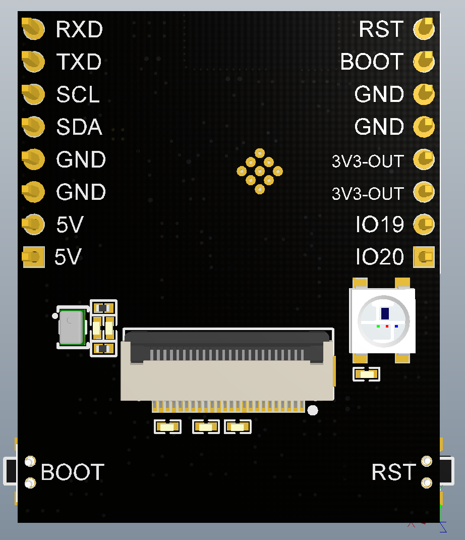
6.1 USB to Serial
| Parameter | Specification |
|---|---|
| Chip | CH340K |
| USB interface | USB-C (USB1) |
| Serial connection | TXD→U0RXD (IO44), RXD→U0TXD (IO43) (crossed) |
| USB matching resistors | R4, R5 22R/1% (in series with D+/D-) |
| DTR/RTS | One-click flashing auto-controls BOOT + EN |
6.2 One-Click Download Circuit
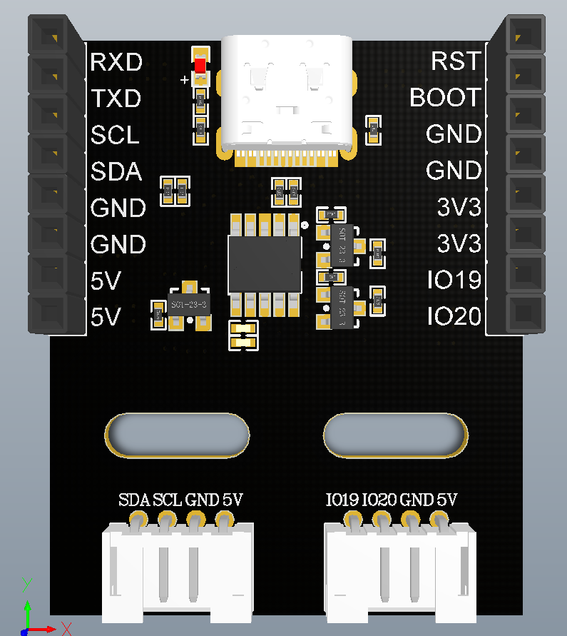
Uses Q1 and Q2 (S8050 NPN transistors) for automatic flashing:
| CH340K Signal | Control | Target Pin |
|---|---|---|
| DTR | → Q1 → | ESP32 EN (CHIP_PU) |
| RTS | → Q2 → | ESP32 BOOT (IO0) |
Principle: the USB flashing tool toggles DTR/RTS to automatically control the BOOT and EN sequence — no manual button presses required.
6.3 Core Board ↔ Base Board Connector Pin Table
| Base Board Pin | Core Board Pin | Signal Name | ESP32 GPIO | Function |
|---|---|---|---|---|
| P1-1 | P1-1 | VDD50 | — | 5V power output |
| P1-2 | P1-2 | VDD50 | — | 5V power output |
| P1-3 | P1-3 | GND | — | Power ground |
| P1-4 | P1-4 | GND | — | Power ground |
| P1-5 | P1-5 | SDA | IO41 | I2C data (shared with camera/ES8311) |
| P1-6 | P1-6 | SCL | IO42 | I2C clock (shared with camera/ES8311) |
| P1-7 | P1-7 | U0TXD | IO43 | Serial port 0 transmit (connects to CH340K RXD) |
| P1-8 | P1-8 | U0RXD | IO44 | Serial port 0 receive (connects to CH340K TXD) |
| P2-1 | P2-1 | ESP_P | IO20 | USB differential data positive (D+) |
| P2-2 | P2-2 | ESP_N | IO19 | USB differential data negative (D-) |
| P2-3 | P2-3 | VDD33 | — | 3.3V power output |
| P2-4 | P2-4 | VDD33 | — | 3.3V power output |
| P2-5 | P2-5 | GND | — | Power ground |
| P2-6 | P2-6 | GND | — | Power ground |
| P2-7 | P2-7 | BOOT | IO0 | Boot mode / flashing |
| P2-8 | P2-8 | CHIP_PU | EN | Chip reset control |
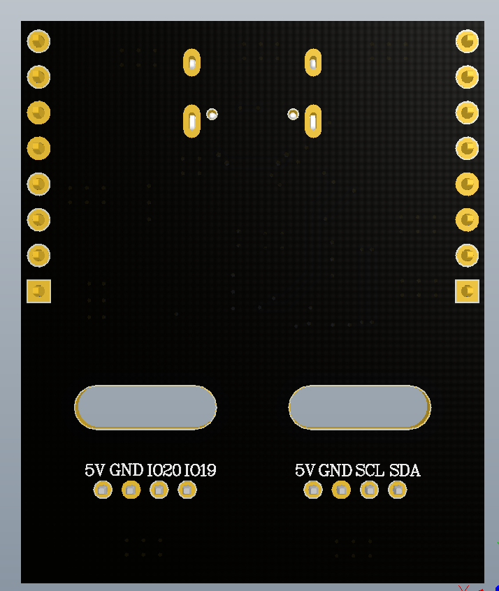
6.4 Base Board Expansion Interfaces
| Interface | Exposed Signals | Purpose |
|---|---|---|
| P3 (I2C, 4Pin) | 5V1, GND, SDA, SCL | External I2C devices |
| P4 (UART, 4Pin) | 5V1, GND, ESP_P, ESP_N | External USB/serial devices |
7. Complete GPIO Usage Table
Total: 33 GPIOs occupied, about 8 GPIOs available.
| GPIO | Function | Signal | Notes |
|---|---|---|---|
| IO0 | BOOT | BOOT | Boot mode / flashing (S2 button, 10K pull-up + 0.1μF debounce) |
| IO1 | DVP D2 | CAM_Y4 | Pixel data bit2 |
| IO2 | DVP D1 | CAM_Y3 | Pixel data bit1 |
| IO3 | DVP D3 | CAM_Y5 | Pixel data bit3 |
| IO4 | DVP D0 | CAM_Y2 | Pixel data bit0 |
| IO5 | DVP D4 | CAM_Y6 | Pixel data bit4 |
| IO6 | DVP PCLK | CAM_PCLK | Pixel clock input |
| IO7 | DVP D5 | CAM_Y7 | Pixel data bit5 |
| IO8 | DVP D6 | CAM_Y8 | Pixel data bit6 |
| IO9 | DVP XCLK | CAM_XCLK | Camera master clock (24MHz) |
| IO10 | DVP D7 | CAM_Y9 | Pixel data bit7 |
| IO11 | DVP HREF | CAM_HREF | Line sync |
| IO12 | DVP PWDN | CAM_PWDN | Camera power-down control |
| IO13 | DVP VSYNC | CAM_VSYNC | Frame sync |
| IO14 | DVP RESET | CAM_RESET | Camera reset |
| IO18 | WS2812 | RGB_LED_DIN | WS2812 RGB LED data input |
| IO19 | USB differential | D- (ESP_N) | USB differential data negative (D-) |
| IO20 | USB differential | D+ (ESP_P) | USB differential data positive (D+) |
| IO21 | WS2812 DOUT | RGB_LED_DOUT | WS2812 cascade output (available when not cascaded) |
| IO29 | SPI CS | Flash_CS | External Flash chip select |
| IO30 | SPI SCLK | Flash_CLK | External Flash clock |
| IO31 | SPI SO | Flash_DO | External Flash data output |
| IO32 | SPI SI | Flash_DI | External Flash data input |
| IO33 | SPI HOLD | Flash_HOLD | External Flash Hold |
| IO34 | SPI WP | Flash_WP | External Flash write protect |
| IO38 | I2S BCLK | I2S_BCLK | ES8311 bit clock |
| IO39 | I2S MCLK | I2S_MCLK | ES8311 master clock |
| IO40 | I2S DIN | I2S_DIN | ES8311 ADC data input |
| IO41 | I2C SDA | I2C_SDA | Shared by camera + ES8311 + external I2C |
| IO42 | I2C SCL | I2C_SCL | Shared by camera + ES8311 + external I2C |
| IO43 | UART0 TX | UTXD | Serial port 0 transmit (base board CH340K) |
| IO44 | UART0 RX | URXD | Serial port 0 receive (base board CH340K) |
| IO47 | I2S WS | I2S_WS | ES8311 word select (LRCK) |
| IO48 | I2S DOUT | I2S_DOUT | ES8311 DAC data output |
| EN | CHIP_PU | RST/EN | Enable/reset (S1 button, 10K pull-up) |
Available GPIOs (unoccupied, expandable)
| GPIO | Feature | Suggested Use |
|---|---|---|
| IO15 | General-purpose IO | Expansion |
| IO16 | General-purpose IO | Expansion |
| IO17 | General-purpose IO | Expansion |
| IO35 | General-purpose IO | Expansion |
| IO36 | General-purpose IO | Expansion |
| IO37 | General-purpose IO | Expansion |
| IO45 | General-purpose IO | Expansion |
| IO46 | General-purpose IO | Expansion |
⚠️ Occupied GPIOs: 0,1,2,3,4,5,6,7,8,9,10,11,12,13,14,18,19,20,21,29,30,31,32,33,34,38,39,40,41,42,43,44,47,48
Available: 8 GPIOs
8. Key Design Constraints
8.1 I2S Peripheral Configuration
- The ESP32-S3 has two I2S controllers:
- I2S0: assigned to the ES8311 codec (MCLK=IO39, BCLK=IO38, WS=IO47, DOUT=IO48, DIN=IO40), bidirectional I2S Duplex, supporting recording and playback simultaneously
- ES8311 I2C control: SDA=IO41, SCL=IO42, device address 0x30
8.2 DVP and I2S DMA Coexistence
- DVP uses the LCD_CAM peripheral's DMA channel
- ES8311 uses I2S0 DMA (single bidirectional I2S interface)
- The two do not conflict, but pay attention to PSRAM bandwidth (8MB PSRAM is sufficient)
- GPIO45/46 have no audio connection and can be used for other purposes; GPIO47 is used for I2S WS
8.3 I2C Bus Sharing
- IO41 (SDA) + IO42 (SCL) connect to both the camera and the external I2C interface
- I2C pull-up resistors: R12 (SDA, 4.7K/1%), R13 (SCL, 4.7K/1%), pulled up to VDD33
- Make sure the camera's I2C address does not conflict with external devices
- OV2640 default I2C address: 0x60 (write) / 0x61 (read) — no conflict with the ES8311 (0x30)
8.4 Sufficient Flash Capacity
- 16MB Flash — ample space, enough to support:
- OTA dual-partition scheme (factory + ota_0 + ota_1)
- SPIFFS for the Web admin panel (~1MB)
- XiaoZhi AI multilingual resource packs (.p3 files)
- NVS configuration partition
- Reserved space for upgrades
- No need to worry about firmware size; the multi-Agent AI fits entirely
8.5 DVP Camera Input Pin Constraints
- D0-D7, VSYNC, HREF and PCLK are input pins, driven by the camera sensor
- When developing the driver, make sure these pins are configured in INPUT mode only
- The I2S audio pins (38,39,40,47,48) can be configured as outputs (supported by the ESP32-S3)
9. ESP-IDF Configuration Recommendations
9.1 Key sdkconfig Items
Plaintext
# 芯片
CONFIG_IDF_TARGET_ESP32S3=y
CONFIG_ESP32S3_DEFAULT_CPU_FREQ_240=y

# Flash (16MB)
CONFIG_ESPTOOLPY_FLASHSIZE_16MB=y
CONFIG_ESPTOOLPY_FLASHMODE_QIO=y
CONFIG_ESPTOOLPY_FLASHFREQ_80M=y

# PSRAM (8MB Octal)
CONFIG_SPIRAM=y
CONFIG_SPIRAM_MODE_OCT=y
CONFIG_SPIRAM_SPEED_80M=y
CONFIG_SPIRAM_MALLOC_ALWAYSINTERNAL=4096
CONFIG_SPIRAM_MALLOC_RESERVE_INTERNAL=49152
CONFIG_MBEDTLS_EXTERNAL_MEM_ALLOC=y

# Cache
CONFIG_ESP32S3_INSTRUCTION_CACHE_32KB=y
CONFIG_ESP32S3_DATA_CACHE_64KB=y
CONFIG_ESP32S3_DATA_CACHE_LINE_64B=y

# 摄像头
CONFIG_CAMERA_MODULE_CUSTOM=y
CONFIG_CAMERA_PIN_XCLK=9
CONFIG_CAMERA_PIN_PCLK=6
CONFIG_CAMERA_PIN_VSYNC=13
CONFIG_CAMERA_PIN_HREF=11
CONFIG_CAMERA_PIN_SIOD=41
CONFIG_CAMERA_PIN_SIOC=42
CONFIG_CAMERA_PIN_PWDN=12
CONFIG_CAMERA_PIN_RESET=14
CONFIG_CAMERA_PIN_Y2=4
CONFIG_CAMERA_PIN_Y3=2
CONFIG_CAMERA_PIN_Y4=1
CONFIG_CAMERA_PIN_Y5=3
CONFIG_CAMERA_PIN_Y6=5
CONFIG_CAMERA_PIN_Y7=7
CONFIG_CAMERA_PIN_Y8=8
CONFIG_CAMERA_PIN_Y9=10
CONFIG_CAMERA_XCLK_FREQ=24000000

# 音频 (ES8311 Codec, I2S0)
# ES8311 I2S: MCLK=39, BCLK=38, WS=47, DOUT=48, DIN=40
# ES8311 I2C: SDA=41, SCL=42, addr=0x30
9.2 Camera Configuration
C
// esp32-camera 引脚配置
camera_config_t config = {
    .pin_pwdn  = 12,
    .pin_reset = 14,
    .pin_xclk  = 9,
    .pin_siod  = 41,
    .pin_sioc  = 42,
    .pin_d7    = 10,
    .pin_d6    = 8,
    .pin_d5    = 7,
    .pin_d4    = 5,
    .pin_d3    = 3,
    .pin_d2    = 1,
    .pin_d1    = 2,
    .pin_d0    = 4,
    .pin_vsync = 13,
    .pin_href  = 11,
    .pin_pclk  = 6,
    .xclk_freq_hz = 24000000,
    .pixel_format = PIXFORMAT_RGB565,  // 或 PIXFORMAT_JPEG
    .frame_size   = FRAMESIZE_QVGA,    // 320x240
    .jpeg_quality = 12,
    .fb_count     = 2,
    .fb_location  = CAMERA_FB_IN_PSRAM,
    .grab_mode    = CAMERA_GRAB_WHEN_EMPTY,
};
Next Steps
- Quick Start — flash, network connection and AI mode switching in five steps
- Serial Protocol Manual — complete AT command reference